The semiconductor world could be on the brink of a significant transformation, with new findings from researchers detailing an innovative approach to modulating the polarity of Bi2O2Se (BOSe) thin films. This breakthrough hinges on an area-selective doping method using zinc ions, pitting BOSe against traditional silicon in next-generation electronic device fabrication.
Since its discovery in 2017, BOSe has captured scientists' attention due to its air stability and high electron mobility, making it an attractive candidate as the semiconductor landscape evolves. However, unlike silicon, the challenge has always lay in achieving effective p-type doping, a crucial characteristic for complementary circuits within transistors.
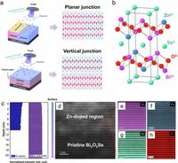
Here, researchers have developed a pulsed laser doping method that operates at a relatively low temperature of around 600 K. This innovation, they suggest, represents a robust technique that is compatible with standard back-end processing in semiconductor manufacturing.
"Our results help promoting the application of this material system towards the development of the next-generation electronics," wrote the authors of the article, highlighting the importance of this technique in paving the way for practical applications.
The traditional methods of doping often resulted in structural damage to the semiconductor material, undermining the ongoing integrity of the devices. In contrast, the newly introduced pulsed laser method utilizes a 248 nm wavelength laser, ensuring limited damage while effectively introducing Zn2+ ions into the BOSe lattice. The researchers found that these ions substitute for Bi3+ sites within the structure, fostering a hole-dominating feature that is essential for establishing p-type conductivity.
According to the insights gleaned from experimental results, the device exhibits both planar and vertical structures, showcasing the versatility of the BOSe semiconductor platform. In particular, the vertical p-n junction created demonstrated an impressive on/off photoresponse ratio exceeding 106 when exposed to green light at a wavelength of 532 nm.
The advantageous properties of the resulting BOSe-based vertical p-n junction extend beyond its conductivity; researchers observed that it could achieve an incredible responsivity and detectivity, with measurements reaching approximately 1.1E13 Jones.
The ability to create n- and p-type homojunctions through refined methods like pulsed laser doping represents a significant leap towards the deep integration of 2D materials in practical electronic applications. Existing silicon architectures impose limitations as transistor technologies progress towards smaller nodes, undermining performance consistency across devices.
Moreover, the research team thoroughly examined the structural features of doped BOSe materials using various advanced characterization techniques. Analysis revealed clean, sharp interfaces critical for high-performing electronic devices, enabling the various layers—doped and undoped—of BOSe to work in concert without compromising lateral and vertical integration.
Notably, the vertical geometric configuration offered enhanced performance benefits by enabling the separated photogenerated carriers and significantly amplifying responsivity in reasonable testing conditions.
"The electronic potential of n- and p-type BOSe can be resolved, and the current measurements show rectification behavior characteristic," wrote the authors of the article, emphasizing the key findings from the electrical characteristics of the p-doped BOSe homojunctions.
The achievements of this research not only highlight the significant advancements in semiconductor technology but also underline the importance of 2D materials like BOSe in potentially replacing silicon. As electronic devices evolve, the complete integration of these advanced materials could foster a new generation of energy-efficient and high-performance electronics capable of meeting the demands of modern technology.
In conclusion, the ability to tune the polarity and performance of BOSe through selective doping may reveal exciting future paths for semiconductor development, bearing implications for the Internet of Things (IoT), flexible electronics, and other emergent technologies. As the scientific community continues exploring the unchartered capabilities of low-dimensional materials, next-generation electronics could become remarkably versatile and efficient, edging closer to the epitome of modern integrated circuits.