Researchers have unveiled a novel method for constructing multilayer artificial excitonic crystals using a stacking technique known as the “2N method,” which dramatically enhances the optical properties of two-dimensional transition metal dichalcogenides (TMDCs). This innovative approach allows for the creation of a 16-layer MoS2 crystal, which retains its monolayer-like excitonic properties and achieves remarkable improvements in light absorption and emission.
The transition to using artificial crystals made from TMDCs—materials that show significant potential in optoelectronic devices—is aimed at overcoming the limitations posed by traditional methods of creating multilayer structures. The newly described 2N method simplifies the process by enabling the fabrication of N-layer crystals through only a number of stacking operations, effectively addressing interlayer interactions that can diminish excitonic responses in thicker materials.
“The challenges of maintaining excitonic properties in bulk structures are complex,” explained the authors of the article, emphasizing the breakthrough of weakly coupled multilayers. This enables researchers to preserve the advantageous properties of monolayer materials while scaling up their applications for practical use.
Significantly, the fabricated 16-layer MoS2 crystal exhibited extraordinary increases of up to 643% and 646% in absorption and photoluminescence (PL) features, respectively. The discovery marks a substantial leap in the capability of manipulating optical properties within created crystals.
Beyond MoS2, the research team also developed a superlattice comprising alternating layers of WSe2 and MoS2. This configuration displayed up to a 400% increase in quadrupolar interlayer exciton emission compared to dipolar excitons observed in previous bilayer counterparts. The precise control of interlayer alignment—achieved using a novel fabrication technique involving self-cracked silicon wafers and nickel sacrificial layers—was essential for this development.
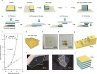
The researchers synthesized a centimeter-scale monolayer MoS2 crystal on a sapphire substrate before employing the 2N stacking method. This process incorporates exact interlayer alignment—critical for sustaining the favorable excitonic behaviors that would typically be lost in bulk materials.
The optical intensity of the 16-layer structure increased steadily, achieving a maximum second harmonic generation (SHG) signal, 35 times higher than that of monolayer samples. Thanks to this new method, which allows for easy manipulation of layer thickness and stacking arrangements, the researchers were able to yield multilayers without needing extensive heating processes. Such features are vital for future applications in photonic and optoelectronic systems.
Moreover, not all methods of constructing multilayered structures are equal. Previous techniques resulted in reduced excitonic responses due to increased interlayer interaction and alterations in energy band structure. “The significance of our findings underscores the effectiveness of the 2N method,” stated the authors of the article.
The study also delved into the excitonic dynamics within the constructed crystals. Upon testing, PL intensity across the different layered regions demonstrated an unexpected increase in emission strength, contrasting starkly with traditional TMDC layers—wherein more layers typically result in reduced excitonic emission. With the assembled 16-layer crystal, researchers recorded over 300 times stronger integrated PL intensity compared to the bulk 2H-MoS2, indicative of preserved monolayer-like attributes.
This research represents a promising frontier for developing advanced optoelectronic applications, as the enhanced excitonic responses offer pathways for improved efficiency in devices that rely on these two-dimensional materials. The findings may pave the way for scalable production methods that can employ complex van der Waals structures in various optoelectronic technologies.
While the new 2N method shows great promise, ongoing research aims to refine this technique further and explore its potential for constructing hybrid moiré and ferroelectric crystals, enhancing the capabilities of artificial crystals and their future applications in the field.