Recent advances in the synthesis of two-dimensional materials have led to the development of large-scale, high-quality WSe2 films, a key component for the next generation of electronic devices. Using an innovative alkali-assisted chemical vapor deposition (AACVD) method, researchers have successfully grown monolayer and bilayer WSe2 films that show significantly low defect densities. This improvement promises to enhance the performance of WSe2 transistors, making them viable candidates for scalable, high-performance electronic applications.
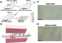
The study, published in Nature Communications, outlines how the AACVD method utilizes potassium hydroxide (KOH) to facilitate nucleation on sapphire substrates. This technique allows for the controlled growth of monolayer and bilayer WSe2 films, achieving defect densities as low as 1.6 × 10^12 cm−2 for monolayers and 1.8 × 10^12 cm−2 for bilayers.
"This newly developed method allows us to grow 2-inch monolayer and centimeter-scale bilayer WSe2 films, which are crucial for their applications in transistors," the authors of the article noted. The remarkable quality of these films enables impressive electronic mobility, with the bilayer WSe2 displaying hole/electron mobilities of 119/34 cm²/Vs and monolayers achieving mobilities of 105/22 cm²/Vs.
WSe2, or tungsten diselenide, is regarded as an attractive material for both p-type and n-type channels in scaled transistors due to its ability to provide high electron and hole mobilities. However, until now, the growth of high-quality WSe2 films has been challenging due to the need for low defect densities across large areas. Traditional chemical vapor deposition (CVD) methods often failed to yield the desired film quality.
One of the main challenges with WSe2 is the relatively low vapor pressure of its precursors, which complicates the large-area growth of uniform films. Various strategies have been attempted in the past, including the addition of halogen salts or plasma-enhanced techniques, but these often resulted in films of inferior quality.
To improve this, the researchers implemented an AACVD process. By placing KOH and H2WO4 in separate crucibles during the reaction, they ensured a controllable introduction of precursors at specific temperatures, thus optimizing the nucleation process. This method also allows for adjustments to be made for varying substrate conditions, like miscut sapphire surfaces, which are essential for achieving bilayer WSe2 films.
The bilayer WSe2 transistors created through this process show not only lower contact resistance for both n-type and p-type materials but also improved performance metrics when compared to their monolayer counterparts. The reduced electron injection barriers related to the lower conduction band edge energy of bilayer WSe2 enhances overall device efficiency.
Notably, this research highlights the potential of bilayer WSe2 for advanced implementations in electronics, particularly as the industry pushes towards smaller, more efficient devices. The low defect density of 1.8 × 10^12 cm−2 positions bilayer WSe2 favorably as a strong contender in the race for next-generation transistors capable of extending the limits of current semiconductor technology.
The researchers used state-of-the-art techniques, including scanning transmission electron microscopy (STEM) and scanning tunneling microscopy (STM), to characterize the films and to analyze defects thoroughly. These investigations revealed point defects primarily identified as oxygen substitutions, a valuable insight for engineers aiming to optimize the efficiency and performance of WSe2 in real-world applications.
As the field of two-dimensional materials continues to evolve, the growth techniques and findings from this study mark a significant milestone. There is a clear path forward for both the enhancement and scaling of WSe2 transistors in the context of integrated circuit design and development—ensuring that performance remains aligned with the desperate pace of semiconductor miniaturization dictated by Moore's Law.